Aller au contenu principal
IJL
Top bar
Accès
Annuaire
Contact
Espace media
Espace membres
HAL
fr
en
Search
Search
Saisir les termes à rechercher.
cnrs
ul
Toggle navigation
Main navigation
Laboratoire
Actualités
Agenda
Présentation
Thématiques de recherche
Départements scientifiques
Services supports
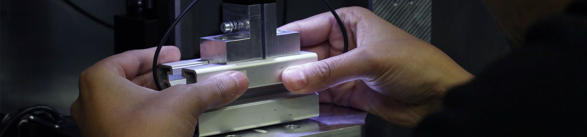
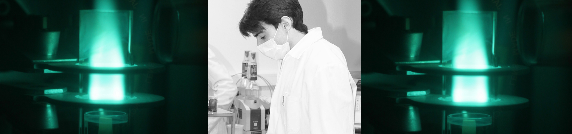
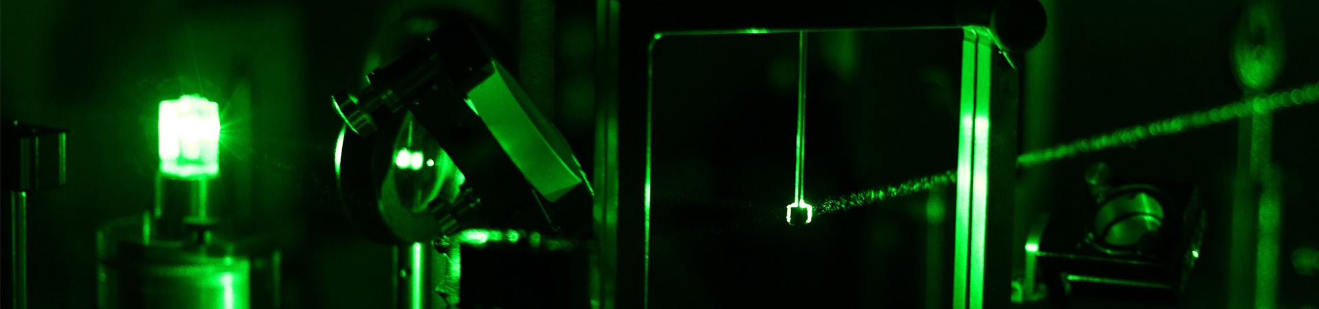
Parc instrumental
Publications sur HAL
Thèses du laboratoire
Equipes
Projets & partenaires
Projets de recherche
Partenaires publics
Collaborations académiques
Affiliations & réseaux
Centres de Compétences
Conception et Fabrication (CC Héré)
Diffraction, Diffusion, Fluorescence et Tomographie X, Spectroscopie Mössbauer (CC X-Gamma)
Dépôts et Analyses sous Ultravide de nanoMatériaux (CC D.A.U.M.)
Informatique et Calcul (CC ERMIONE)
Magnétisme et Cryogénie (CC MagCryo)
Micro et Nanotechnologies (CC MiNaLor)
Microscopies, Microsondes et Métallographie (CC 3M)
Optique-Lasers (CC OL)
Offre entreprises
Présentation et contact
Nos compétences
Nos technologies
Nos prestations
Start-ups
Ils nous font confiance
Formation & emploi
Masters
Ecoles d'ingénieurs
Doctorat
Formation professionnelle
Travailler à l'IJL
Offres d'emploi
Grand public & Media
Evénements tout public
Actions pour élèves et enseignants
Expositions
Le Tube D.A.U.M. en réalité virtuelle
Prix & nominations
Espace media
bandeau
Previous
Next
A la une
[Publication dans Nature] Des solides cristallins à faible conductivité thermique
Lire la suite
[Nomination] Badreddine Assouar devient membre de l'Académie Européenne des Sciences
Lire la suite
[Prix] Javier Quilez Bermejo obtient le Prix de la Société Francophone d'Etude des Carbones 2023
Lire la suite
[article] L’art de façonner la structure de bandes électroniques des semi-conducteurs
Lire la suite
[Prix et distinction] Cécile Floer reçoit le prix Edouard Branly
Lire la suite
Previous
Next
Thématiques de recherche
Matériaux
Métallurgie
Nanosciences
Plasmas
Surfaces
Electronique
Energie
Environnement
Industrie du futur
Mobilité
Préservation des ressources
Santé
Agenda
Date
13 mai 2024
Type d'événement
Colloque
COLLOQUE SFEC 2024
Lire la suite
Date
29 mai 2024
Type d'événement
Colloque
Conférence ASFGD 2024
Lire la suite
Date
06 juin 2024
Type d'événement
Conférence
Conférence SFP
Lire la suite
Date
18 novembre 2024
Type d'événement
Conférence
Conférence internationale IEEE sur les circuits et systèmes électroniques (ICECS)
Lire la suite
Rejoignez l'IJL !
Rejoignez l'IJL !
Chiffres clés
600
Instruments de recherche
25
Equipes de recherche
300
Articles par an dans des revues à comité de lecture
167
Chercheurs et enseignants-chercheurs
177
Doctorant.e.s
105
Personnels support
60
Nationalités
30
Pays partenaires
32
Soutenances de thèse par an
Previous
Next
Dernières publications
Voir toutes les publications