[Article] Heavily doped Si nanocrystals for infrared plasmonics
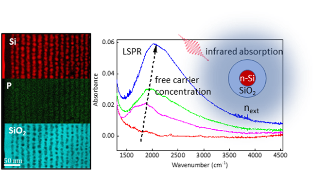
As building blocks of multifunctional materials involving coupling at the nanoscale, highly doped semiconductor nanocrystals are of great interest for potential applications in nanophotonics. In this work, we investigate the plasmonic properties of highly doped Si nanocrystals embedded in a silica matrix. These materials are obtained by evaporation of heavily phosphorus-doped SiO/SiO2 multilayers in an ultrahigh vacuum chamber followed by rapid thermal annealing. For P contents between 0.7 and 1.9 atom %, structural investigations at the nanoscale give clear evidence that P atoms are mainly located in the core of Si nanocrystals with concentrations reaching up to 10 atom %, i.e., well beyond the solid solubility limit of P in bulk Si. Alloying and formation of SiP nanoparticles are observed for P contents exceeding 4 atom % in the multilayer. Infrared absorption measurements give evidence of a localized surface plasmon resonance located in the 3−6 μm range. A core−shell structure was used to model Si nanocrystals embedded in a silica matrix. Based on the Mie theory and the Drude model, both the mobility and the free charge carrier density were extracted from the simulation, with values reaching 27 cm2 V−1 s−1 and 2.3 × 1020 cm−3, respectively. This results in a dopant activation rate of about 8%.

Authors
Alix Valdenaire, Alaa Eldin Giba, Mathieu Stoffel, Xavier Devaux, Loic Foussat, Jean-Marie Poumirol, Caroline Bonafos, Sonia Guehairia, Rémi Demoulin, Etienne Talbot, Michel Vergnat, Hervé Rinnert
References
ACS Applied Nano Materials 2023, 6, 3312-3320
DOI
